
Understanding Peak Currents of Isolated Gate Drivers
When deciding which gate driver to use for a given application, one frequently asked question is: what is the maximum current that a driver can deliver?
Peak current is a critical parameter in gate driver data sheets. This metric is commonly regarded as the end-all and be-all of gate driver drive strength. The time it takes to turn on and off a MOSFET/IGBT is related to the current that the gate drive optocoupler can deliver, but it does not tell the entire story.
Peak current is so commonly used in the industry that it appears in the title of many gate driver data sheets. Regardless, its definition varies from section to section. This article discusses the issues with using peak current as a deciding factor when selecting a gate driver for a specific application, as well as comparing some of the more common peak current representations in data sheets.
A comparison of gate drivers with similar peak current numbers in their titles is investigated, as is a discussion of gate drive strength.
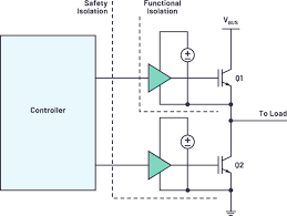
Example Application
In order to operate power devices, isolated gate drivers provide level shifting, isolation, and gate drive strength. The isolated nature of these smart gate drivers enables high-side and low-side device driving, as well as the provision of a safety barrier if a suitable device is used.`
A suitable isolated gate driver must be able to reproduce the timing presented on the primary side and drive the power device’s gate fast enough to allow for acceptable switching transitions. Faster switching transitions can result in lower switching losses, so the ability to switch quickly is frequently valued.
In general, the greater the power a power device can handle within one type of switch technology, the greater the load it presents to the gate drive optocoupler.
Isolated gate drive optocoupler are frequently used in half-bridge configurations, as illustrated in Figure 2. The high-side driver must be able to swing between system ground and VBUS voltage while providing the required drive strength to the power device it is driving.
Load Consideration
The switching speed of a MOSFET/IGBT is determined by the time required to charge or discharge the gate. An external series gate resistor is used in practice to tune the gate voltage rise/fall times and share power dissipation with the gate driver IC.
The RC circuit shown in Figure 3 is obtained by modeling the power device as a capacitor and the gate driver as a MOSFET output stage running through an external series gate resistor. In this simplified model, IPK SRC = VDD/(RDS(ON) P + REXT) and IPK SNK = VDD/(RDS(ON) N + REXT) are the source and sink peak current equations. REXT is set to 0 for a short-circuit peak current measurement, but an external series resistor is present in application.
Where:
The gate driver NMOS’s on resistance is RDS(ON) N.
The gate driver PMOS’s on-resistance is RDS(ON) P.
The external series gate resistor is denoted by REXT.
CGATE EQUIV represents the power device’s equivalent capacitance.
Power Dissipation: A Major Consideration
A power device’s gate must be charged and discharged, which requires the expenditure of energy. If the equivalent capacitance model is used and the gate is fully charged and discharged each switching cycle, the power dissipated by the gate switching action for gate drive optocoupler is:
Where:
The power dissipated in one cycle of switching the gate is denoted by PDISS.
The equivalent gate capacitance is denoted by CEQ.
The total voltage swing of the power device gate is denoted by VDD2.
The total gate charge of the power device is denoted by QG TOT.
The switching frequency of the system is denoted by fS.
It should be noted that the equivalent gate capacitance, CEQ, is not the same as the CISS found on power device data sheets.
It is frequently 3 to 5 times greater than CISS, and the total gate charge, QG TOT, is a more precise number to use. It should also be noted that the series resistance of charging and discharging is not included in this equation because it only refers to the total power dissipated in the switching action and not the power dissipated within the gate drive optocoupler IC specifically.
Given the isolated nature of gate drive optocoupler , standards require that different isolation regions be separated by adequate creepage and clearance distances. Any galvanic conductors in the primary to secondary region path reduce creepage and clearance distances, so exposed pads or heat slugs for isolated gate drive optocoupler are extremely rare.
This means that one of the primary methods for lowering integrated circuit thermal resistance is no longer available, emphasizing the importance of shifting power dissipation outside of the isolated gate drive optocoupler package to allow for higher ambient temperature operation at a given operating point.
The thermal resistance of the package used is roughly related to the pin count, internal metallization, lead frame connections, and package size because isolated gate drive optocoupler cannot be heated.
When comparing available parts for a given isolated gate drive optocoupler part number, the package size, pin count, and often pinout will be the same, resulting in roughly the same theta-JA numbers.
The internal junction temperature rises due to thermal dissipation within the gate drive optocoupler IC. The power dissipation calculated in Equation 1 is the total power dissipated by raising and lowering the power device gate.
The internal resistances of the output drive FETs, RDS(ON) N and RDS(ON) P, and the external series gate resistor, REXT, dissipate the power dissipated within the gate drive optocoupler IC.
If the gate drive optocoupler mostly operates in the linear region, the power dissipation ratio experienced by the gate drive optocoupler IC is:
If RDS(ON) N = RDS(ON) P = RDS(ON), Equation 2 can be simplified to:
The total power experienced by the gate drive optocoupler IC as a result of the power device switching is then Equation 1 multiplied by Equation 3:
In equation 4, a smaller RDS(ON) results in a smaller portion of the power dissipation occurring within the isolated gate drive optocoupler . To achieve the desired rise/fall time, the RC constant for charging and discharging the power device gate must be preserved:
The series combination of the internal RDS(ON) and the external series gate resistor results in the resistance in the RC constant.
In other words, if two competing gate drive optocouplers with the same rise and fall speeds are used in the same application, the driver with the lower RDS(ON) allows for a larger external series gate resistor while maintaining the total series resistance constant, resulting in less power dissipation within the gate drive optocoupler IC itself.
Conclusion
Since the source and sink current ratings are reported differently, forming an opinion about the drive strength of different parts based on a cursory glance at the data sheet heading can be misleading. This lack of transparency in the peak current definition can cause a part to be oversold or undersold, reducing its chances of being chosen for a specific application before it is thoroughly evaluated at the customer end.
It is critical for a fair comparison to ensure that the peak currents mentioned in data sheets are compared like-for-like. When evaluating isolated gate drive optocouplers, consider the importance of thermal headroom and low RDS(ON). Although two gate drive optocouplers can be tuned to the same rise and fall values, selecting the driver with the lower RDS(ON) provides more thermal headroom and greater switching speed flexibility.


